Surface Cleanliness Detection of Silicon Substrates by the BeVision M1 Static Image Analyzer
2025-01-09Application Note
The cleanliness of the substrate surface is crucial to the quality and performance of the material that grows on it. The BeVision M1 static image analyzer provides powerful support for the detection of surface cleanliness of silicon substrate materials, greatly saving detection time and labor costs.
| Product | BeVision M1 |
| Industry | Electronics and Semiconductors |
| Sample | Silicon Substrates |
| Measurement Type | Surface Cleanliness |
| Measurement Technology | Static Image Analysis |
Jump to a section:
- Importance of Surface Cleanliness
- Automatic Scanning and Panoramic Stitching Functions of BeVision M1
- Case study: surface cleanliness detection of silicon substrates
- Conclusion
Importance of Surface Cleanliness of Silicon Substrate Materials
In the semiconductor industry, the surface cleanliness of silicon substrate materials is crucial. As the foundation for integrated circuit manufacturing, even tiny contaminants on the surface of silicon substrates can have a serious impact on subsequent processes. An immaculate surface can ensure the smooth progress of key processes such as thin film deposition and lithography and improve the performance and yield of devices. For example, if there are particulate contaminants on the surface, it may lead to short circuits or open circuits in the circuit; organic contaminants may affect the adhesion of the film. Therefore, thoroughly detecting the surface cleanliness of silicon substrate materials is a key link in ensuring the quality of semiconductor products.
![]()
Figure 1. A silicon substrate
Automatic Scanning and Panoramic Stitching Functions of BeVision M1 Static Image Analyzer
The BeVision M1 static image analyzer provides powerful support for the detection of surface cleanliness of silicon substrate materials, greatly saving detection time and labor costs. Equipped with a metallographical microscopy and high-speed CMOS camera, the substrate's surface can be precisely magnified and observed. The BeVision M1 can automatically scan the surface of the substrate, identify and classify defects and impurities based on the size and shape. At the same time, the captured local images can be seamlessly stitched into a full-view image, allowing users to clearly and intuitively observe the surface condition of the entire sample surface.
To avoid being out of focus during scanning, the intelligent auto-focusing function can evaluate the clarity of images in real-time and automatically adjust focus when the clarity fall below the standard to guarantee the imaging quality. BeVision M1 helps to discover tiny defects (down to 0.3μm) and contaminated areas that may be overlooked, providing a strong guarantee for accurately evaluating surface cleanliness.
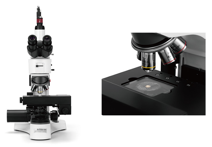
Figure 2. The BeVision M1 image analyzer
Case study: surface cleanliness detection of silicon substrates
a.The panoramic scanning
The silicon substrate was automatically scanned through the panoramic analysis mode. Images were precisely stitched to a panorama, in which edge particles were stitched at the pixel level, ensuring no particle was distorted or lost. Figure 3 displays the panoramic image of the substrate surface.
![]()
Figure 3. The panoramic image of the silicon substrate
Table 1. Particle count based on size (μm)
| Color | xA(μm) | Count | Percentage |
| 7cfc00 | <10.00 | 37 | 63.79% |
| fe00fe | 10.00 - 20.00 | 17 | 29.31% |
| ffff00 | 20.00 - 50.00 | 3 | 5.17% |
| ff4500 | >50.00 | 1 | 1.72% |
Particles on the panoramic image can be classified and identified in different colors based on up to 34 size and shape characteristics such as area-equivalent diameter (xA), Feret diameter, aspect ratio, circularity, and so on. Table 1 shows the particle count and percentage of impurities in each size class on the silicon substrate surface. This substrate had 1 pcs impurity over 50 μm marked in red, 3 pcs between 20~50 μm marked in yellow, 17 pcs between 10~20 μm marked in purple, and 37 pcs smaller than 10 μm marked in green.
Generaly, particles of defects smaller than 50 μm can't be seen with naked eyes. The thickness of the film that grows on the substrate is usually micrometer-level or even nanometer-level, thus the micrometer-level impurities or defects would deteriorate the quality and performance of the film.
Besides particle classification, it's also able to search particles by overlaying multiple size and shape parameters. Table 2 shows there were 2 pcs impurities or defects on the substrate surface within the size of 20~50 μm and the aspect ratio of 0~0.7.
Table 2. Particle count based on size and shape parameters
| Particle Attributes | Minimum | Maximum |
| Aspect Ratio | 0.000 | 0.700 |
| xA | 20.000 | 50.000 |
| Count | 2 | |
| Percentage | 3.45% |
Figure 4 shows the size distribution and shape information. The smallest impurities is close to 1 μm, and the largest one is close to 100 μm. With shape information, users can analyze the type of the defects or impurities, such as fibers, dots, scratch, etc. The BeVision software offers number-weighted, area-weighted and volume-weighted distributions for option.
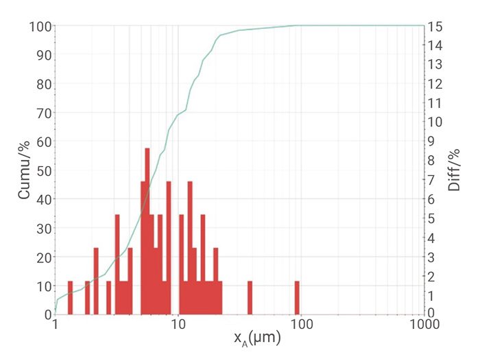
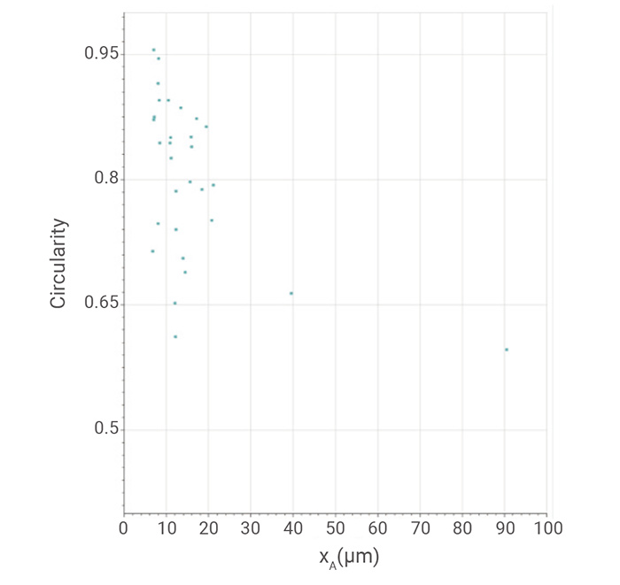
Figure 4. The size distribution

Figure 5. shows the extracted single-particle images of impurities or defects.
b.Local re-scanning
After a full-view scanning and getting the impurity distribution on the substrate surface, to further inspect and analyze one or some of them, a local re-scanning with a higher magnification was performed by directly selecting a smaller area on the panorama as shown in Figure 6 (up). Through the magnified rescanning, the small dot that was boxed was maginified, as shown in Figure 6 (bottom).
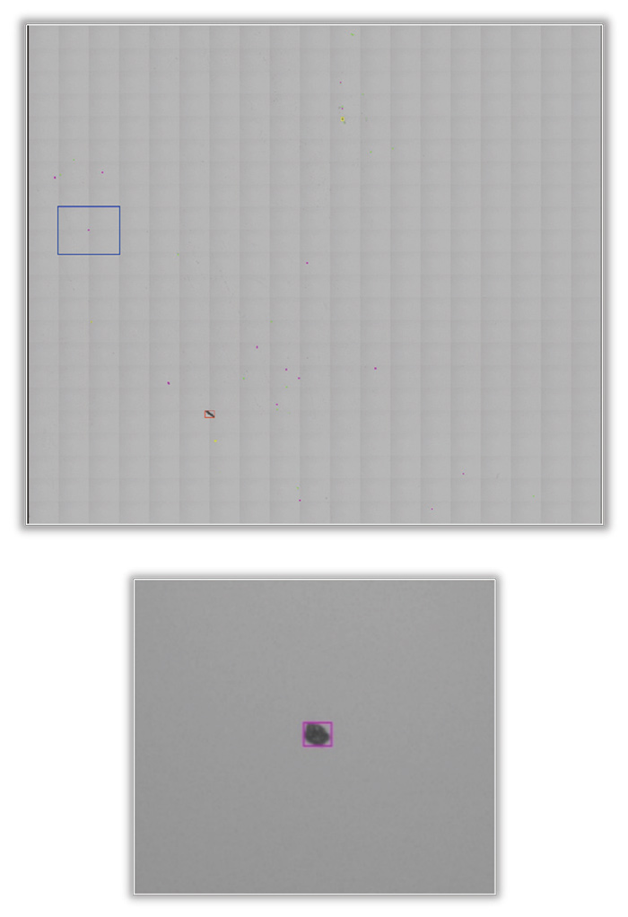
Figure 6. The panoramic image (up) and the local image of re-scanning (bottom)
Table 3 shows size and shape results of the re-scanned particle.
Table 3. The size and shape results of the re-scanned particle
|
Area |
240.171 |
L/W Ratio |
1.230 |
|
Perimeter |
21.230 |
Ellipse Ratio |
0.876 |
|
xA |
17.487 |
Aspect Ratio |
0.751 |
|
xP |
19.490 |
Elongation |
0.961 |
|
Long Diameter |
19.731 |
Straightness |
1.000 |
|
Short Diameter |
16.048 |
lrregularity |
0.770 |
|
xFmax |
21.142 |
Compactness |
0.827 |
|
xFmin |
15.883 |
Extent |
0.715 |
|
xLF |
19.964 |
Box Ratio |
0.757 |
|
xLmax |
19.821 |
Circularity |
0.897 |
|
xLmin |
17.360 |
Solidity |
0.952 |
|
xMmax |
20.799 |
Convexity |
0.992 |
|
xMmin |
15.807 |
Concavity |
0.048 |
Conclusion
The cleanliness of the substrate surface is crucial to the quality and performance of the material that grows on it. BeVision M1 static image analyzer can automatically scan the substrate surface, providing a full view of the substrate surface and particle classification based on size and shape.
The intelligent auto-focusing during scanning ensures the clarity of each image. The pixel-level image stitching precision guarantees accurate particle count and size measurement. The BeVision software offers not only 34 size and shape characteristics but also automatic functions to help easily and deeply analyze the results. BeVision M1 offers a powerful tool to make the cleanliness inspection easier, more efficient and deeper.
About the Author
 |
Echo Cao Application Engineer @ Bettersize Instruments |
|
|
BeVision M1 Image Analyzer
|
Rate this article

