
Electronics and Semiconductors
Instruments provided by Bettersize offer particle size and shape analyses of the raw materials of electronic products.
In the electronics industry, many materials and processes have strict requirements for particle size and particle shape. For example, the silicon carbide powder used for cutting silicon wafers requires a tight particle size distribution and a sharp particle shape corner angle, the cerium oxide abrasive used for polishing requires a small particle size without large particles, and the silica dioxide materials used for sealing integrated circuits require strict standards for the particle size distribution and spherical degree. Particle size and particle shape analysis is a basic method of production and product quality guarantee in the electronics industry.
During the research, design, manufacturing and quality control of electronic components, the instruments provided by Bettersize can help you to realize material properties, including:
● Guaranteeing CMP slurry quality.
● Guaranteeing particle size and particle shape of milling for cutting and polishing.
● Guaranteeing the quality of integrated circuit sealing materials.
Curated Resources
Related Particle Size Analyzer
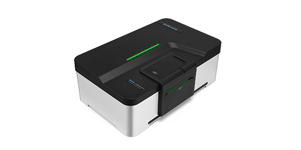
BeNano 180 Zeta Pro
Nanoparticle Size and Zeta Potential Analyzer
Technology: Dynamic Light Scattering, Electrophoretic Light Scattering, Static Light Scattering
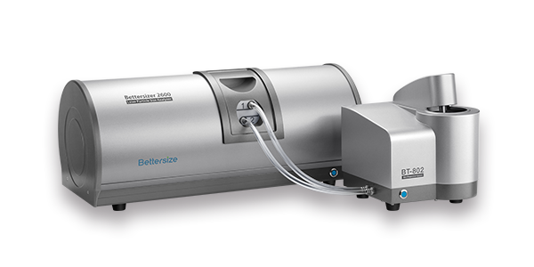
Bettersizer 2600
Laser Diffraction Particle Size Analyzer
Measurement range: 0.02 - 2,600μm (Wet)
Measurement range: 0.1 - 2,600μm (Dry)
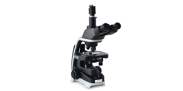
BeVision M1
Automated Static Image Analyzer
Dispersion type: Dry
Measurement range: 1 - 10,000μm
Technology: Automated Static Image Analysis
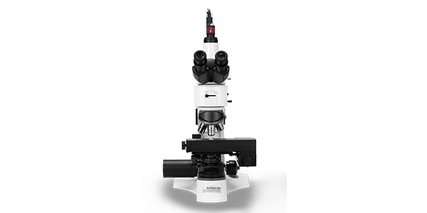
BeVision S1
Classical and Versatile Static Image Analyzer
Dispersion type: Dry & Wet
Measurement range: 1 - 3,000μm
Technology: Static Image Analysis
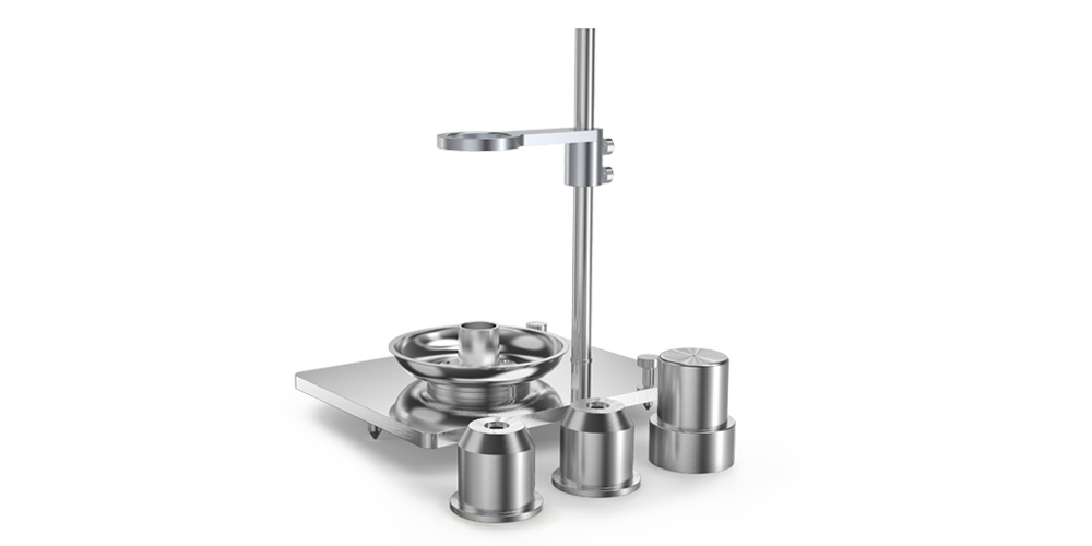
BeDensi B1
Bulk Density Tester
Measurement: Bulk Density
Compliance with GB/T 16913
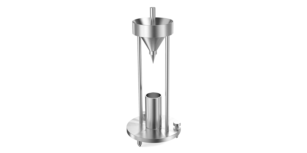
HFlow 1
Flowmeter Funnel
Measurement: Bulk density and Flow rate
Compliance with USP, Ph. Eur., ASTM, and ISO standards